Designing a Chip with the Drag-and-Drop Editor
This tutorial will guide you through creating your very first quantum chip layout using the visual, drag-and-drop schematic editor.
Step 1: Open the Schematic Editor
On the main navigation sidebar, click on the Schematic Editor button.
The page will load a large visual design workspace consisting of a component library panel on the left, a main grid canvas in the center, and a properties panel on the right.
What this means: The Schematic Editor is a visual environment where you can design quantum processors by arranging physical components on a chip instead of writing raw code.
Step 2: Understand the Component Library
The left-hand panel is the Component Library. Here, you will find standard quantum structures:
Qubits: The basic building blocks of a quantum processor that store quantum information. In this product, these are superconducting qubits (such as Transmon Crosses or Transmon Pockets) represented by crosses or pockets on metal.
Resonators: Special metal lines (like coils or loops) placed next to qubits. They are used to measure the state of the qubit (readout).
Routes / Transmission Lines: Planar metal wires that connect qubits to each other or to external signals.
Feedlines: Shared microwave signal lines used to read out multiple qubits at once.
Launchpads: Large metal contact pads located on the edge of the chip where external cabling is wire-bonded to communicate with the chip components.
What this means: The library contains all pre-designed physical models you need to construct a functional chip layout.
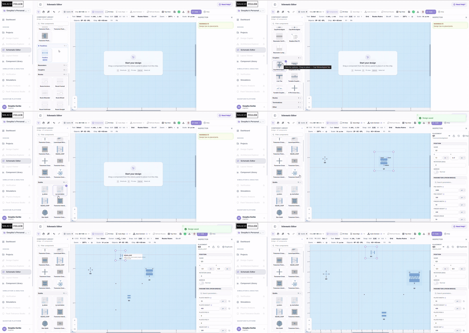
Step 3: Drag a Component onto the Canvas
Look at the Component Library on the left.
Click on the Qubits section to expand it.
Click and hold your mouse button on a component, such as Transmon Cross or Transmon Pocket.
Drag your mouse cursor onto the main grid Canvas in the center.
Release the mouse button to drop the component onto the grid.
What you just did: You placed a physical qubit model onto the chip substrate. You will see a visual representation of the qubit outline appear on the canvas grid.
Step 4: Arrange, Connect, and Delete Components
Move a component: Click on a component on the canvas and drag it to a new location on the grid.
Connect components: 1. Hover your cursor over one of the connection ports (called pins) on the edge of a component. 2. Click and drag a line from that pin to a pin on another component. 3. Release the mouse button to complete the connection (this creates a transmission line or coupler).
Delete a component: 1. Click on a component on the canvas to select it. 2. Press the Delete or Backspace key on your keyboard, or click the Delete (trash can) button on the editor toolbar.
What you just did: You customized the processor’s topology (how qubits connect to each other). Connecting qubits is necessary for them to exchange information.
Magic Pencil — Auto Connect 
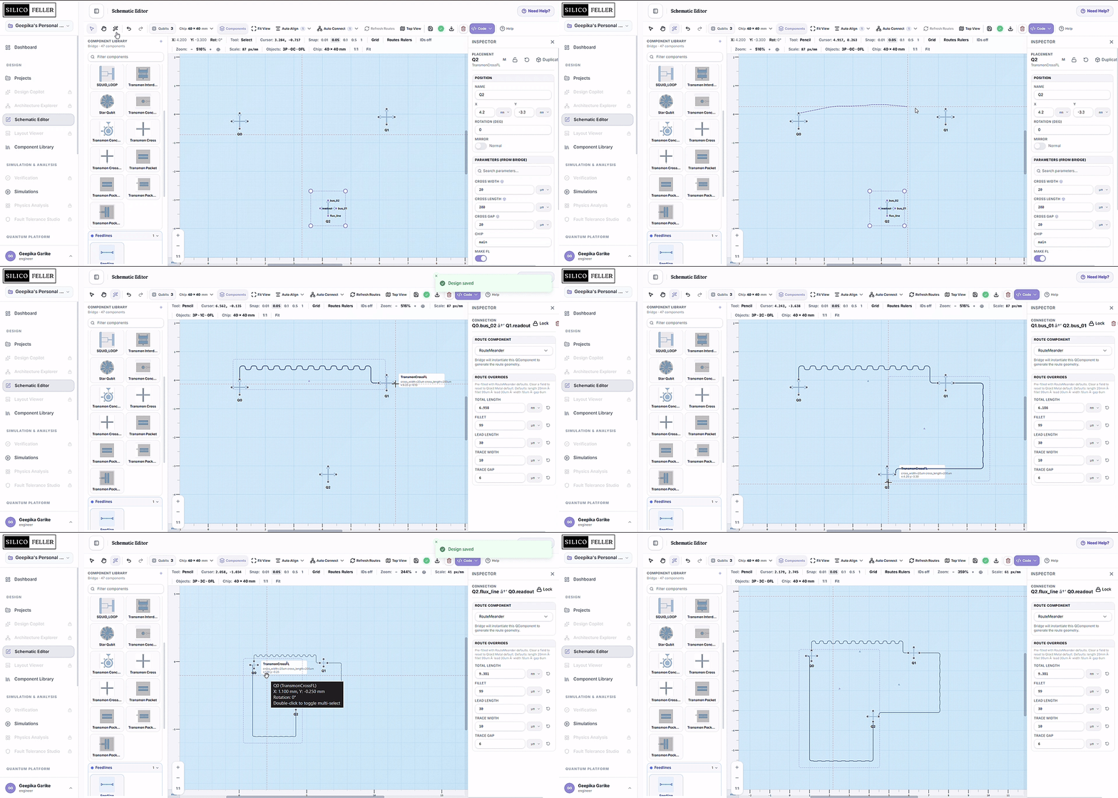
The Magic Pencil (also called Auto Connect) is a one-click tool that automatically generates topology connections between all qubits on your canvas — no manual pin-dragging required. Instead of drawing each transmission line by hand, you pick a topology pattern and the editor instantly wires all qubits together using the correct route components.
How to use Magic Pencil:
Place two or more qubit components on the canvas (see Step 3).
Click the Auto Connect button in the toolbar. A dropdown menu appears.
Choose one of the available topology patterns (see table below).
The editor instantly draws route connections between all qubits in that pattern.
Optional: Select specific qubits first (click or Ctrl+click) to auto-connect only the selected subset.
Available topology patterns:
| Pattern | Description |
|---|---|
| Grid | Balanced rows × columns layout — the most common rectangular arrangement. |
| Horizontal | Single row, connected left to right. |
| Vertical | Single column, connected top to bottom. |
| Rhombus | Diamond / rhombus pattern — useful for symmetric 4-qubit cells. |
| U-Shape | Three sides connected, open at the bottom — common for readout chains. |
| Circle | Equidistant ring connecting all qubits in a loop. |
| H-Shape | Two staggered rows — the heavy-hex topology used in IBM Quantum processors. |
| Linear Chain | Spatial nearest-neighbour chain based on actual qubit positions on the canvas. |
| Star | Hub + spokes — one central qubit connected to all others. |
What this means: Magic Pencil saves hours of manual wiring. Once connected, each route is a real RouteMeander component with editable parameters — you can still fine-tune lengths, gaps, and turns in the Property Inspector after auto-connecting.
Step 5: Edit Component Properties
Click on any component (such as a qubit or resonator) placed on the canvas.
Look at the Property Inspector panel on the right side of the screen.
You will see several input fields showing dimensions and parameters:
pos_x and pos_y: The exact coordinates of the component on the chip.
frequency_ghz: The target operating frequency of the qubit or resonator.
junction: Parameters of the Josephson junctions (the superconducting elements inside the qubit).
Change any value (for example, type a new position or change the frequency) and press Enter or click Save.
What this means: Editing these parameters changes the physical and electrical specifications of the component, which directly affects how it performs in simulations.
Step 6: Save and Export Your Design
Look at the toolbar at the top of the editor.
Click the Save button to save the current chip layout to your project files.
Click the Export button to download your design as a standardized layout description file (such as GDS or JSON).
What you just did: You saved your work to the cloud and exported the physical description of the chip, which can now be simulated or fabricated.